Multilayer Communication PCB

Multilayer Communication PCB
– The Heart of Modern Connectivity
In today’s interconnected world, the demand for seamless, efficient communication systems has never been higher. A Communication PCB (Printed Circuit Board) plays a crucial role in making this possible by serving as the backbone of devices that enable everything from wireless data transfer to satellite communication. This specialized PCB is engineered to handle high-frequency signals, ensuring that information is transmitted accurately and at high speeds across various communication networks. From consumer electronics to industrial applications, Communication PCBs are a vital component in telecommunications, IoT devices, and numerous wireless technologies, ensuring that devices remain connected, responsive, and reliable.
A high-quality Communication PCB must meet stringent requirements, including the ability to handle high data rates, reduce signal interference, and maintain consistent performance in diverse environments. With rapid advancements in 5G, IoT, and cloud computing, Communication PCBs must also evolve to accommodate higher frequency ranges, enhanced signal integrity, and greater durability, thus playing an integral part in modern, high-performance communication systems.
Specifications for a Communication PCB:
1. Material and Construction
- Substrate Material: FR4, Rogers, or high-frequency laminates for signal integrity.
- Copper Thickness: Ranges from 1oz to 3oz, depending on the power requirements.
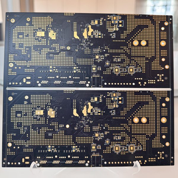
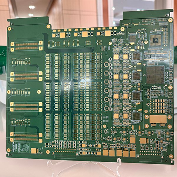
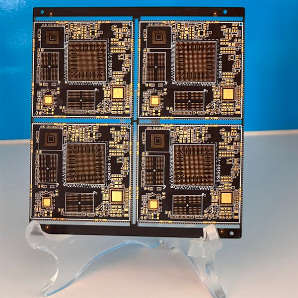
- Layers: Multi-layer design, typically 4-12 layers for improved functionality and compactness in high-frequency applications.
- Surface Finish: ENIG (Electroless Nickel Immersion Gold) or HASL (Hot Air Solder Leveling) for excellent solderability and durability.
2. Signal Handling and Frequency
- Frequency Range: Designed to handle high frequencies from 1 GHz up to 10 GHz or more, suitable for Wi-Fi, Bluetooth, and cellular applications.
- Impedance Control: Precision impedance control to minimize signal loss and reflection, ensuring signal integrity across high-speed channels.
- Differential Pairs: Supports differential pair routing for high-speed, low-interference data transmission.
3. Power and Ground Layers
- Dedicated Ground and Power Layers: Separate layers for grounding and power to reduce noise and improve signal clarity.
- Power Integrity: Designed for optimal power distribution to ensure stable performance of communication components.
4. Thermal Management
- Thermal Conductivity: High thermal conductivity materials for efficient heat dissipation in high-power applications.
- Heat Sinks and Vias: Built-in heat sinks and thermal vias to manage temperature, ensuring consistent operation and preventing overheating.
5. Environmental Resistance
- Operating Temperature Range: -40°C to +85°C or more for use in a variety of conditions.
- Humidity Resistance: Coatings and laminates resistant to moisture to protect from environmental impact.
- EMI Shielding: Built-in features to shield against electromagnetic interference, ensuring reliable data transmission.
6. Compliance and Standards
- Certification: Compliant with industry standards such as IPC Class 2 or Class 3, depending on the application.
- RoHS and REACH Compliance: Environmentally friendly and compliant with international safety and material standards.
Technique Capability:
Layer Count | From 2L to 24L |
Material | CEM-3. FR4. High High CTI Halogen Free |
Thickness | Inner: 0.1mm Outer. 0.3-3.5mm |
Copper Thickness & UL | 1/3 OZ, H/H OZ, 1/1 OZ, 2120Z, 3/30Z, 4/40Z, 5/50Z |
Working Panel Size | 760mm x 660mm |
Drill Capability | Blind//buried via, Semi-drill, Finished hole size: 0.15mm -6.5mm; NPTH: ±O.05mm PTH: ±0.075mm Hole Position: ±0.075mm |
Trace width/space | 0.05/0.05mm |
Finishing | OSP. LF HAL, Flash Gold. ENIG. Immersion Tin. (Gold Plating) (Carbon Ink) |
Solder mask | Thickness >= 10um (UV Solder Mask) |
Profile & Tolerance: | Punch, Route, V-CUT; ± 0. 1mm |
Peelable Mask: | Thickness >= 0.3mm |
Warp & Twist: | IPC-A-600G . Max. 0.5% |
Functional Test: | IMPEDENCE, OPEN/SHORT, FLYING PROBE. LOW RESISTANCE TEST; |