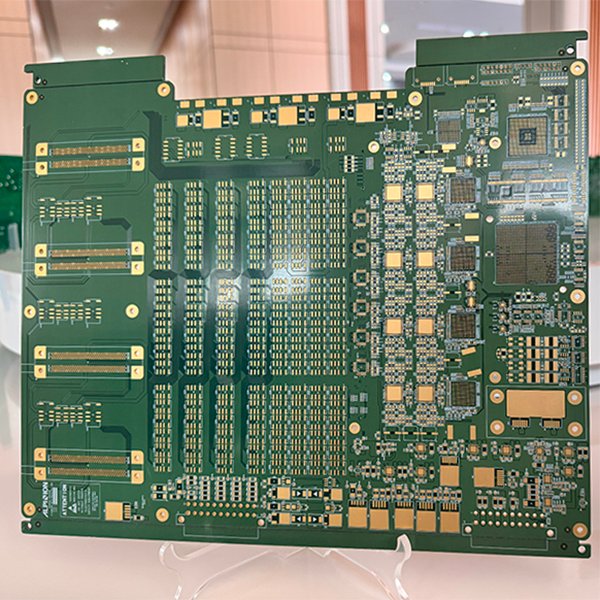
6 Layers PCB
6 Layers with ENIG --- Red soldermask, Min. trace width/space 3/3mil
A 6-layer PCB (Printed Circuit Board) is a multi-layered board that consists of six conductive layers stacked in a specific order. These layers generally include four signal layers and two internal layers dedicated to power and ground planes. The additional layers provide better signal integrity, reduced electromagnetic interference (EMI), and improved heat dissipation compared to simpler PCBs. The layout typically includes alternating signal and plane layers, which allow for compact designs with enhanced functionality.
Applications: 6-layer PCBs are widely used in high-speed and complex electronic applications, such as telecommunications, computing, medical devices, and automotive systems. They are ideal for products requiring high processing power, reliability, and efficient power distribution.
Technique Capability:
Layer Count | From 2L to 24L |
Material | CEM-3. FR4. High High CTI Halogen Free |
Thickness | Inner: 0.1mm Outer. 0.3-3.5mm |
Copper Thickness & UL | 1/3 OZ, H/H OZ, 1/1 OZ, 2120Z, 3/30Z, 4/40Z, 5/50Z |
Working Panel Size | 760mm x 660mm |
Drill Capability | Blind//buried via, Semi-drill, Finished hole size: 0.15mm -6.5mm; NPTH: ±O.05mm PTH: ±0.075mm Hole Position: ±0.075mm |
Trace width/space | 0.05/0.05mm |
Finishing | OSP. LF HAL, Flash Gold. ENIG. Immersion Tin. (Gold Plating) (Carbon Ink) |
Solder mask | Thickness >= 10um (UV Solder Mask) |
Profile & Tolerance: | Punch, Route, V-CUT; ± 0. 1mm |
Peelable Mask: | Thickness >= 0.3mm |
Warp & Twist: | IPC-A-600G . Max. 0.5% |
Functional Test: | IMPEDENCE, OPEN/SHORT, FLYING PROBE. LOW RESISTANCE TEST; |