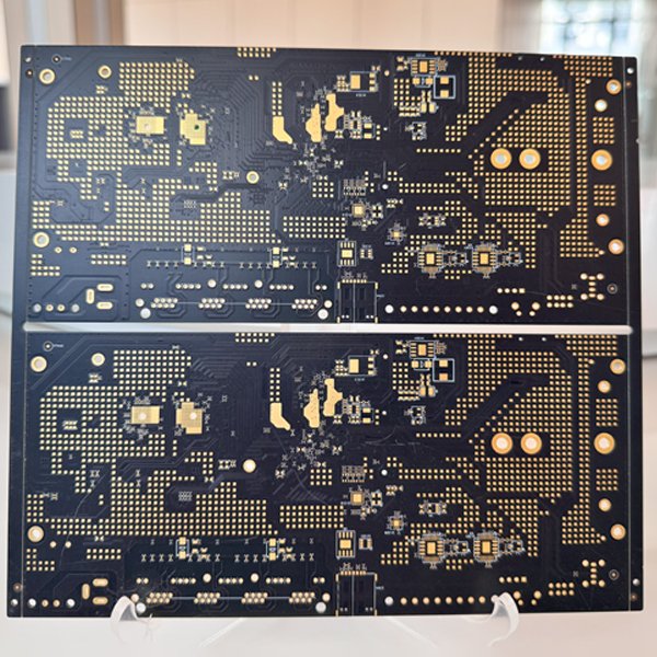
4 Layer PCB with ENIG

4Layers with ENIG
Black soldermask,Minimum drill 0.25mm
This 4-layer PCB features an ENIG (Electroless Nickel Immersion Gold) finish and black soldermask, manufactured to high-precision standards with a minimum drill size of 0.25mm. The board can be produced using industry-standard materials including CEM-3, FR4, and High CTI Halogen Free, with inner layer thickness of 0.1mm and outer layer thickness ranging from 0.3mm to 3.5mm. Supporting multiple copper weight options from 1/3 oz to 5/5 oz, the PCB can be manufactured on panels up to 760mm x 660mm. It offers advanced drilling capabilities including blind/buried vias and semi-drilling, with finished hole sizes ranging from 0.15mm to 6.5mm. The design allows for ultra-fine trace width and spacing down to 0.05mm/0.05mm. Surface finishing options include OSP, LF HAL, Flash Gold, ENIG, Immersion Tin, Gold Plating, and Carbon Ink, with UV soldermask thickness ≥10μm and peelable mask thickness ≥0.3mm. Quality control meets IPC-A-600G standards with maximum warp and twist of 0.5%, and includes comprehensive testing including impedance, open/short, flying probe, and low resistance testing.
Technique Capability:
Layer Count | From 2L to 24L |
Material | CEM-3. FR4. High High CTI Halogen Free |
Thickness | Inner: 0.1mm Outer. 0.3-3.5mm |
Copper Thickness & UL | 1/3 OZ, H/H OZ, 1/1 OZ, 2120Z, 3/30Z, 4/40Z, 5/50Z |
Working Panel Size | 760mm x 660mm |
Drill Capability | Blind//buried via, Semi-drill, Finished hole size: 0.15mm -6.5mm; NPTH: ±O.05mm PTH: ±0.075mm Hole Position: ±0.075mm |
Trace width/space | 0.05/0.05mm |
Finishing | OSP. LF HAL, Flash Gold. ENIG. Immersion Tin. (Gold Plating) (Carbon Ink) |
Solder mask | Thickness >= 10um (UV Solder Mask) |
Profile & Tolerance: | Punch, Route, V-CUT; ± 0. 1mm |
Peelable Mask: | Thickness >= 0.3mm |
Warp & Twist: | IPC-A-600G . Max. 0.5% |
Functional Test: | IMPEDENCE, OPEN/SHORT, FLYING PROBE. LOW RESISTANCE TEST; |