

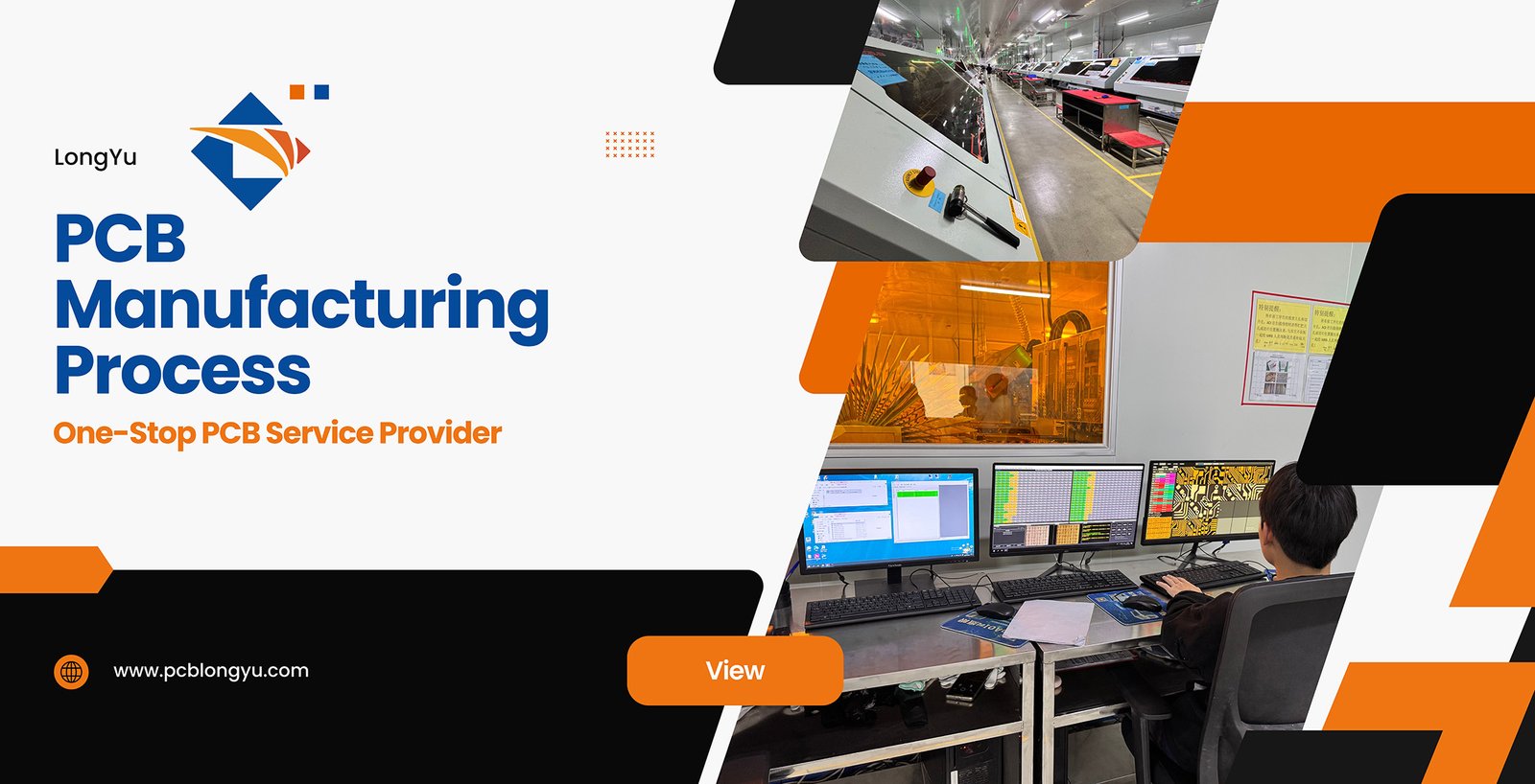
Manufacturing Process at LongYu Technology Co., Ltd.
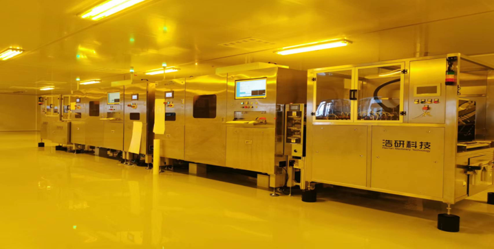
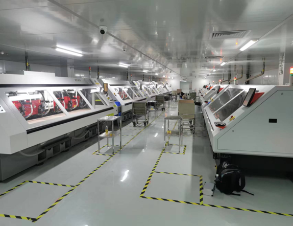
LongYu Technology Co., Ltd. stands as a leader in high-density, multi-layer printed circuit board (PCB) manufacturing, equipped with state-of-the-art facilities and rigorous quality protocols. The factory’s manufacturing process integrates advanced technology and stringent quality checks to ensure precision and reliability at every stage. From initial inner layer preparation to final inspection and packaging, each step is meticulously designed to meet the demands of modern applications across telecommunications, automotive, medical, and industrial sectors. By leveraging automated systems and cutting-edge techniques, LongYu consistently delivers PCBs with superior durability and performance, setting a benchmark in the industry.
Inner Layer Processing: Pre-treatment and Cleaning: The process begins with a cleaning line to prepare the copper panels, ensuring they are free of contaminants. Image Transfer: Laser Direct Imaging (LDI) technology is used to accurately transfer the circuit patterns onto the inner layers. Etching and AOI (Automated Optical Inspection): The panels are etched to create circuit patterns, followed by AOI to detect any defects in the pattern before lamination. |
|
|
|
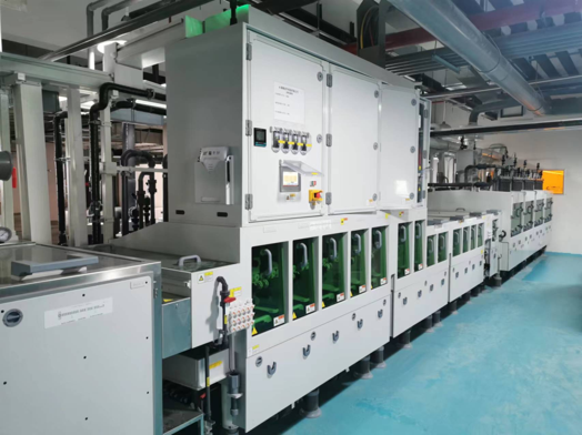
| Lamination: Brown Oxide Treatment: A brown oxide treatment is applied to improve adhesion between layers. Multi-Layer Lamination: The layers are aligned and laminated under high heat and pressure to bond them into a single, multi-layer structure. |
|


| Drilling: Hole Drilling: Precision drilling machines create holes (vias) to connect the inner layers. Zhu Hai Long Yu has over 150 drilling machines with plans to expand to 300. Hole Inspection: Hole position accuracy and consistency are verified to ensure quality. |
|


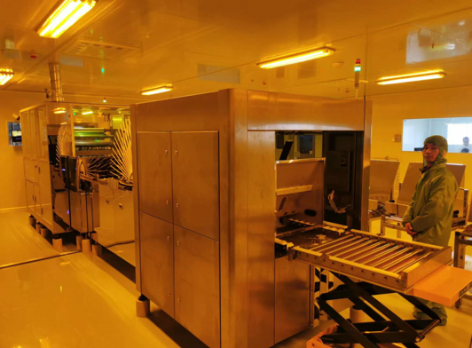
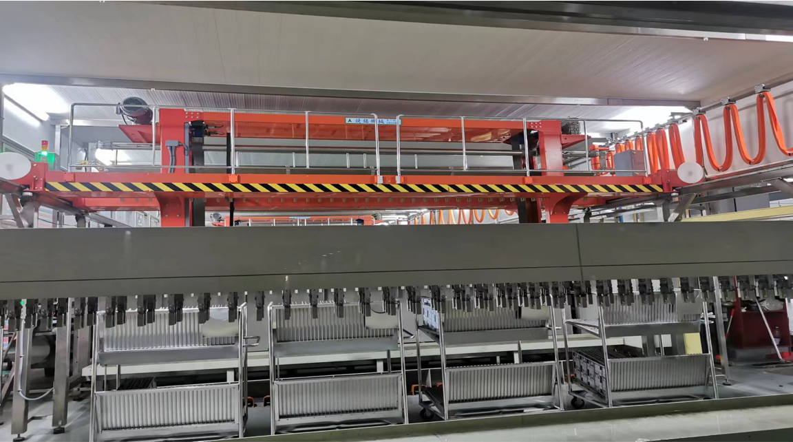
| Plating and Copper Deposition: Panel Plating and Copper Deposition: Using advanced plating lines, copper is deposited onto the drilled holes to create conductive pathways between layers. Pattern Plating: Additional copper is plated onto specific areas to build up trace thickness as required for high-density applications. |
|

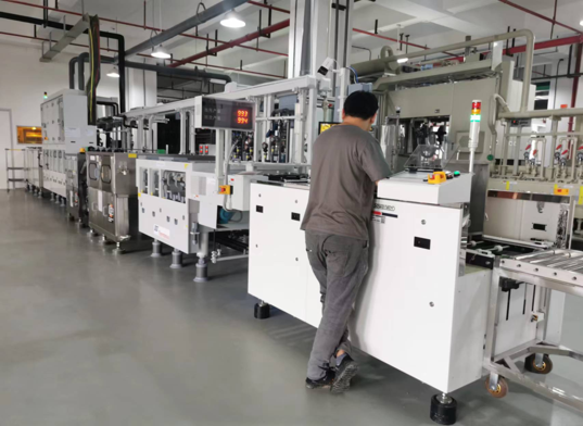
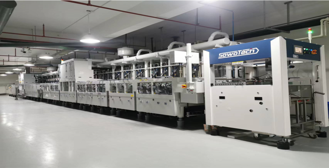
Outer Layer Processing: Imaging and Etching: LDI technology is again used to transfer patterns onto the outer layers, which are then etched to form the external circuitry. Solder Mask Application: A solder mask is applied to protect the copper traces from oxidation and prevent solder bridging during assembly. The factory uses automatic silkscreen printing for precise application. |
|
|
|


Surface Finishing: Surface Treatment Options: To enhance durability and prepare the boards for soldering, various surface finishes are applied based on client requirements. Options include:
|
|
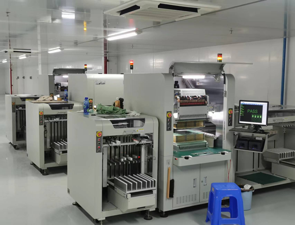
| Testing and Quality Control: Electrical Testing: Extensive testing ensures that the circuits are free of opens and shorts. Flying probe testers and other electrical testers verify each board’s functionality. Reliability and Environmental Testing: Boards undergo reliability testing, including impedance control, high-temperature testing, and solderability assessments. |
|
Summary Table: Key Process Stages:
Process Stage | Description |
| Inner Layer Processing | Pre-treatment, imaging, etching, AOI |
| Lamination | Brown oxide treatment, layer bonding |
| Drilling | Hole drilling, inspection |
| Plating & Copper Deposition | Panel plating, pattern plating |
| Outer Layer Processing | Imaging, etching, solder mask application |
| Surface Finishing | LF HAL, ENIG, Immersion silver, OSP |
| Testing & Quality Control | Electrical testing, reliability checks |
| Final Inspection & Packaging | FQC, automated packaging |
This structured process, supported by advanced equipment and a strong commitment to quality, ensures that LongYu delivers high-quality PCBs suitable for a wide range of applications.