The Evolution of PCB Inspection and Testing Technologies
Printed Circuit Boards (PCBs) are the backbone of modern electronics, enabling the miniaturization and complexity of devices across industries. As PCBs have evolved, so too have the methods to inspect and test them, driven by the need for higher reliability, reduced defects, and compliance with industry standards. This paper explores the historical progression of PCB inspection and testing technologies, from manual methods to AI-driven systems, and evaluates their impact on manufacturing efficiency. A comparative analysis of key technologies, supported by a data table, highlights advancements in defect detection rates, cost-effectiveness, and adaptability to emerging trends like IoT and Industry 4.0.
Introduction
PCBs are critical components in electronics, hosting interconnected circuits that power devices from smartphones to aerospace systems. The complexity of modern PCBs, characterized by high-density interconnects (HDI) and surface-mount technology (SMT), demands rigorous inspection and testing to ensure functionality. Over the decades, inspection methodologies have transitioned from labor-intensive visual checks to automated, data-driven systems. This evolution reflects broader trends in manufacturing: the pursuit of precision, scalability, and integration with smart technologies.
Historical Perspective: Manual Inspection and Basic Testing
In the 1950s–1970s, PCB inspection relied on manual methods. Technicians used magnifying tools and microscopes to identify soldering defects, misalignments, or trace damage. Testing was limited to continuity checks with multimeters or rudimentary bed-of-nails fixtures.
Limitations:
>>> Human error: Defect detection rates averaged 60–70%.
>>> Time consumption: Inspecting complex boards took hours.
>>> Scalability issues: Unsuitable for mass production.
Limitations of Modern PCB Inspection and Testing Technologies
Despite significant advancements, PCB inspection and testing technologies face persistent challenges that hinder universal adoption and optimal performance. A primary limitation is the high cost of advanced systems such as 3D automated optical inspection (AOI) and computed tomography (CT) scanners, which can exceed $1 million, placing them out of reach for small and medium-sized enterprises (SMEs). Additionally, the increasing miniaturization of components, such as 01005-sized resistors (0.4 mm × 0.2 mm) and micro-BGAs, strains even high-resolution imaging systems, leading to inspection blind spots. Hidden or subsurface defects, including voids in solder joints or cracks in multilayer boards, remain difficult to detect without expensive X-ray or CT solutions, which also require specialized operator expertise. While AI-driven systems reduce false positives, they demand substantial computational resources and extensive training datasets to achieve reliability, creating skill gaps in workforce training and data management. Furthermore, technologies like in-circuit testing (ICT) struggle with limited node accessibility in densely packed designs, reducing test coverage. Lastly, the throughput-speed trade-off persists: high-accuracy 3D systems often sacrifice inspection speed, complicating their integration into high-volume production lines. These limitations underscore the need for cost-effective, scalable solutions that balance precision, speed, and adaptability to keep pace with evolving PCB complexity.
The 1980s–1990s: Rise of Automated Optical Inspection (AOI)
The advent of SMT in the 1980s necessitated faster, more accurate inspection. AOI systems emerged, leveraging cameras and image-processing algorithms to scan PCBs for defects like solder bridging or missing components.
Advancements:
>>> Defect detection rates improved to 85–90%.
>>> Throughput: Up to 500 components per minute.
>>> Standardization: Alignment with IPC-A-610 standards for solder quality.
Limitations:
>>> Limited effectiveness on hidden joints (e.g., ball grid arrays).
>>> High false-positive rates requiring human verification.
The 2000s: Automated X-ray Inspection (AXI) and In-Circuit Testing (ICT)
As PCBs incorporated BGAs and chip-scale packages, AOI’s shortcomings prompted the adoption of AXI. X-rays penetrate layers to reveal subsurface defects, such as voids in solder joints. Concurrently, ICT became a staple for post-assembly verification using bed-of-nails testers to check component functionality.
Key Developments in PCB Inspection and Testing Technologies
The evolution of PCB inspection and testing technologies has been marked by transformative advancements that address the growing complexity of electronic assemblies. In the 1980s–1990s, the shift to Surface-Mount Technology (SMT) and miniaturized components necessitated Automated Optical Inspection (AOI), which utilized 2D imaging to achieve defect detection rates of 85–90% and throughputs of 500 components per minute. By the 2000s, the rise of Ball Grid Arrays (BGAs) and hidden solder joints exposed AOI’s limitations, spurring the adoption of Automated X-ray Inspection (AXI). AXI systems, costing 150,000–150,000–500,000, provided 90–95% accuracy in detecting subsurface defects like solder voids. Concurrently, In-Circuit Testing (ICT) became a cornerstone for functional validation, testing 85–95% of component nodes via bed-of-nails fixtures. The 2010s ushered in AI-driven AOI, leveraging machine learning to reduce false positives by 40–60% and boost detection rates to 95–99%, while 3D AOI and Computed Tomography (CT) enabled height measurement and cross-sectional layer analysis for multilayer boards. Industry 4.0 further revolutionized workflows by integrating IoT-enabled analytics, enabling real-time process optimization and predictive maintenance. These advancements, however, introduced challenges, including high costs (e.g., CT scanners exceeding $1 million) and skill gaps in managing AI/ML tools. Today, AI-driven predictive quality systems and cobot-assisted workflows represent the cutting edge, underscoring the industry’s shift toward adaptive, data-centric solutions to meet the demands of next-generation microelectronics and smart manufacturing.
Key Developments:
>>> AXI defect detection: ~95% accuracy for hidden joints.
>>> ICT coverage: 85–95% of component nodes tested.
>>> Cost: AXI systems ranged from 150,000??150,000to500,000, limiting adoption to high-volume manufacturers.
2010s–Present: AI, 3D Imaging, and Industry 4.0 Integration
Recent advancements focus on enhancing precision and predictive capabilities:
AI and Machine Learning
AI-powered AOI systems analyze vast datasets to distinguish between critical defects and benign anomalies, reducing false positives by 40–60%.
3D AOI and Computed Tomography (CT)
3D AOI measures component height and coplanarity, while CT scans provide cross-sectional views for multilayer boards.
IoT and Real-Time Analytics
Industry 4.0 integrates inspection data with production line analytics, enabling predictive maintenance and process optimization.
Comparative Analysis of PCB Inspection Technologies
|
Technology
|
Era
|
Key Features
|
Defect Detection Rate
|
Advantages
|
Limitations
|
Adoption Rate
|
|
Manual Inspection
|
1950s–1970s
|
Visual checks, magnifying tools
|
60–70%
|
Low cost
|
Human error, slow
|
<10% (legacy)
|
|
AOI
|
1980s–2000s
|
Camera-based, 2D imaging
|
85–90%
|
High speed, SMT compatibility
|
Limited to visible defects
|
60% (manufacturing)
|
|
AXI
|
2000s–2010s
|
X-ray imaging, layer penetration
|
90–95%
|
Detects hidden defects
|
High cost, complex analysis
|
30% (high-end)
|
|
ICT
|
1990s–Present
|
Bed-of-nails, electrical testing
|
85–95%
|
Validates component functionality
|
Limited to accessible nodes
|
50% (mixed)
|
|
AI/ML Systems
|
2010s–Present
|
Deep learning, pattern recognition
|
95–99%
|
Low false positives, adaptive learning
|
High computational needs
|
25% (growing)
|
|
3D AOI/CT
|
2010s–Present
|
Height measurement, cross-sectional views
|
97–99%
|
Comprehensive layer analysis
|
Expensive, slow throughput
|
15% (niche)
|
Data Sources: Industry reports (IPC, Grand View Research), 2023 estimates.
Challenges in Modern PCB Inspection
>>> Cost: Advanced systems (e.g., CT scanners) exceed $1M, deterring SMEs.
>>> Skill Gaps: Operating AI/ML tools requires specialized training.
>>> Miniaturization: Components under 01005 size challenge even 3D AOI.
Future Trends
>>> AI-Driven Predictive Quality: Real-time defect root-cause analysis.
>>> Higher-Resolution Imaging: Sub-micron accuracy for microelectronics.
>>> Cobots: Collaborative robots assisting in hybrid inspection workflows.
Here is why choose PCBLongyu
When choosing a PCB manufacturer, reliability and quality are paramount. Here's why PCBLongyu, with its emphasis on superior inspection and testing, stands out:
-
Uncompromising Quality Assurance:
>>> PCBLongyu's commitment to "best PCB Inspection and Testing Technologies" translates to a significantly reduced risk of defects. This means fewer costly errors in your final product.
>>> Rigorous testing throughout the manufacturing process ensures that every PCB meets stringent quality standards.
-
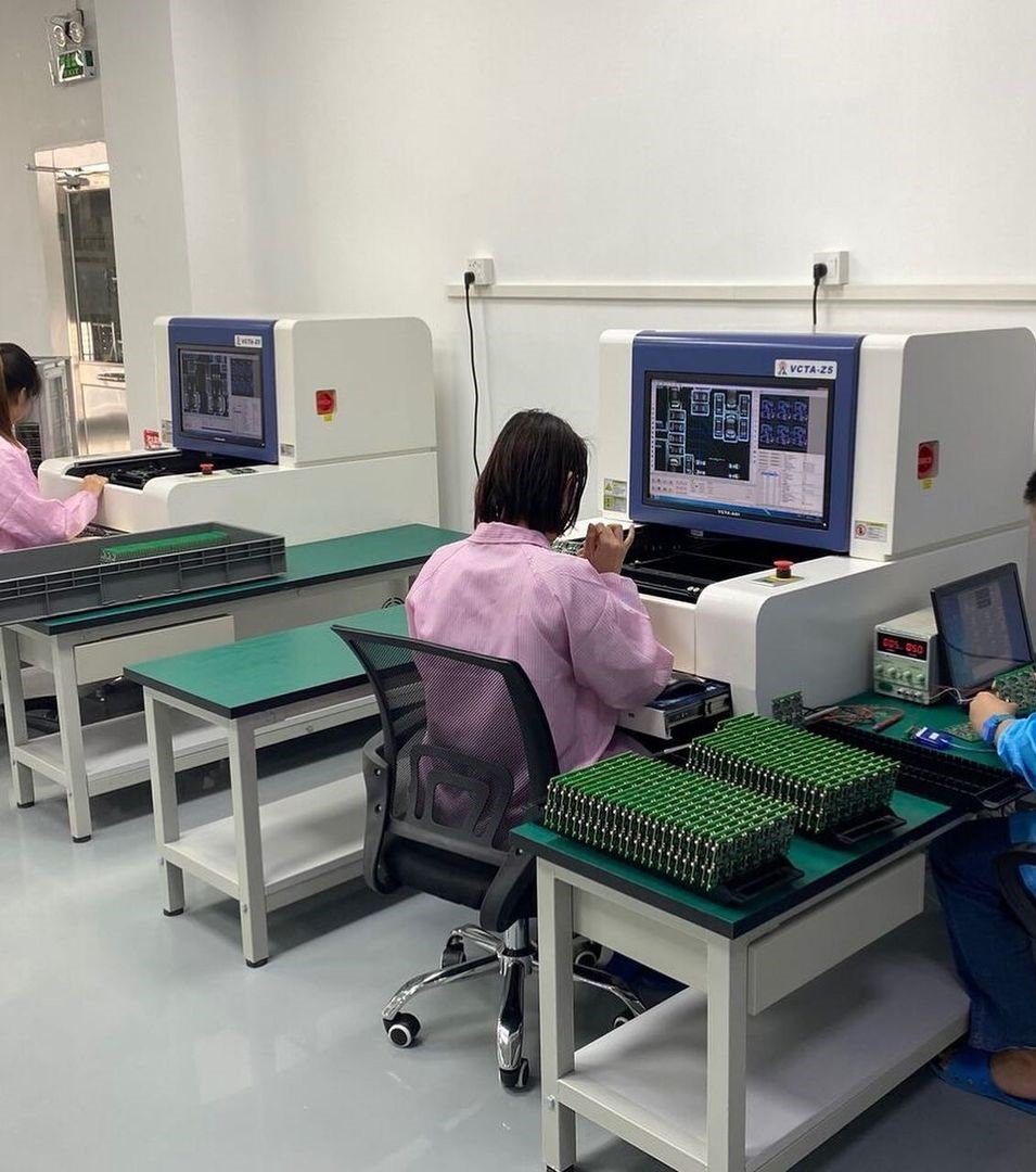
Advanced Inspection Capabilities:
>>> Utilizing cutting-edge inspection technologies like Automated Optical Inspection (AOI), X-ray inspection, and flying probe testing allows PCBLongyu to detect even the most subtle imperfections.
>>> These advanced methods guarantee the precision and reliability of your PCBs.
-
Comprehensive Testing Protocols:
>>> PCBLongyu employs a full suite of electrical testing procedures, including in-circuit testing (ICT) and functional testing, to verify the performance of each PCB.
>>> This comprehensive approach ensures that your PCBs function as intended in their target applications.
>>> Knowing your PCBs have undergone extensive testing provides peace of mind and builds confidence in your final product.
In essence, PCBLongyu's investment in top-tier inspection and testing technologies translates to higher quality PCBs, reduced risk, and greater customer satisfaction.
Conclusion
The evolution of PCB inspection technologies mirrors the electronics industry’s demand for precision and adaptability. From manual checks to AI-enhanced systems, each advancement addresses prior limitations while introducing new challenges. As IoT and smart manufacturing redefine production, inspection technologies will continue to integrate deeper with digital ecosystems, ensuring PCBs meet the reliability standards of tomorrow’s innovations.