In the world of electronics manufacturing, Printed Circuit Boards (PCBs) are the backbone of every device. Whether it's a simple gadget or a complex industrial system, the reliability of the end product heavily depends on the quality of the PCB. However, during mass production, even small defects can lead to large-scale failures, costly recalls, or damage to a brand’s reputation.
Below, we explore some of the most common PCB defects in mass production—and more importantly, how to prevent them.
How Double-Layer PCBs Are Made
A double-layer PCB, also known as a two-layer PCB, has copper traces on both the top and bottom sides of the board. This allows for more complex circuit designs compared to single-layer boards. A double-layer PCB is a type of printed circuit board that has copper traces on both the top and bottom sides. This allows for more complex and compact circuit designs compared to a single-layer PCB, which has copper only on one side. Here is how they are made:
>>> Substrate Preparation: A non-conductive fiberglass (FR4) core is coated on both sides with a thin layer of copper foil.
>>> Photoresist Application: A light-sensitive photoresist is applied to both sides of the board. Then, the circuit pattern is transferred onto the resist using UV light through a photo mask.
>>> Etching: The exposed copper areas (not protected by photoresist) are etched away using chemicals, leaving behind the desired circuit patterns on both layers.
>>> Drilling: Precision drilling machines create vias (small holes) to electrically connect the top and bottom layers. These are called plated through holes (PTH).
>>> Plating: The entire board, including the drilled holes, is plated with copper to create electrical connectivity between the layers.
>>> Solder Mask and Silkscreen: A protective solder mask is applied to insulate the copper traces and prevent short circuits. After that, silkscreen printing adds component labels and markings.
>>> Surface Finish: The board undergoes surface finishing (like HASL, ENIG, or OSP) to enhance solderability and protect copper from oxidation.
>>> Final Testing: Every board is electrically tested (E-test) to ensure there are no shorts or open circuits.
Key Features of Double-Layer PCBs:
>>> Two conductive layers: Top and bottom, both used for routing signals.
>>> Plated Through Holes (PTH): These holes are drilled and plated with copper to electrically connect the top and bottom layers.
>>> More component flexibility: You can place components on both sides of the board.
>>> Higher circuit density: Great for more advanced and space-constrained designs.
Where Are Double-Layer PCBs Used?
v Double-layer PCBs are widely used in:
v Consumer electronics (TVs, radios, speakers)
v Industrial control systems
v Power supplies
v Automotive electronics
v LED lighting systems
v IoT devices
Advantages Over Single-Layer PCBs:
Feature | Single-Layer PCB | Double-Layer PCB |
Copper Layers | 1 side | Both sides |
Circuit Complexity | Low | Medium |
Component Density | Limited | Higher |
Cost | Cheaper | Slightly more expensive |
Applications | Simple devices | Mid-level electronics |
Soldering Defects
Issue: Solder bridges, cold joints, and insufficient solder can lead to open circuits or short circuits.
Prevention:
>>> Use automated solder paste inspection (SPI).
>>> Regularly calibrate reflow ovens.
>>> Choose the right soldering profiles based on board thickness and component density.
Delamination
Issue: Layers of the PCB separate due to trapped moisture or excessive heat.
Prevention:
>>> Bake PCBs before soldering to remove moisture.
>>> Ensure proper lamination pressure and curing time during board fabrication.
>>> Use high-quality base materials.
Misaligned Layers
Issue: In multi-layer boards, layer shifting causes open circuits or shorts.
Prevention:
>>> Invest in high-precision registration systems.
>>> Regularly monitor the alignment process during inner layer bonding.
Insufficient Copper Thickness
Issue: Thin copper traces can lead to overheating or breaking under current load.
Prevention:
>>> Verify copper thickness standards during the design and production stage.
>>> Use impedance control and current-carrying calculations in the design phase.
Component Placement Errors
Issue: Incorrect or skewed component placement affects assembly and functionality.
Prevention:
>>> Utilize high-precision pick-and-place machines.
>>> Implement AOI (Automated Optical Inspection) systems.
>>> Regular operator training and inspection.
Contamination and Residue
Issue: Flux residues or contaminants can corrode connections or affect insulation.
Prevention:
>>> Use no-clean flux or ensure thorough post-solder cleaning.
>>> Maintain a cleanroom environment for assembly.
>>> Inspect boards under UV light or ionic contamination testers.
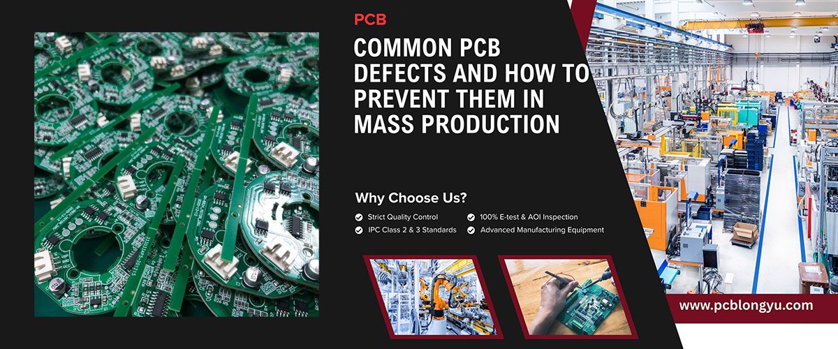
Why Choosing PCBLONGY Can Help You Skip These Mistakes
Mass production comes with high pressure—tight deadlines, bulk quantities, and strict quality expectations. That’s where PCBLONGY stands out as your reliable manufacturing partner.
Here’s how PCBLONGY helps you skip common PCB defects:
>>> 100% E-test & AOI Inspection: Every board goes through electrical testing and optical inspection to catch any potential defect early.
>>> Strict Quality Control: From raw materials to finished products, PCBLONGY applies multiple QC checkpoints to ensure consistency.
>>> Advanced Manufacturing Equipment: High-speed SMT lines, precision drilling, and laser-guided layer alignment reduce human errors and maintain precision.
>>> Engineering Support: PCBLONGY offers DFM (Design for Manufacturability) checks to help clients optimize their designs before production begins.
>>> IPC Class 2 & Class 3 Standards: PCBLONGY follows international standards, ensuring your boards are built to perform under critical conditions.
>>> On-Time Delivery: A smooth production workflow means your PCBs are delivered fast—without quality compromise.
Final Thoughts
Mass production doesn’t mean mass mistakes. By understanding the most common PCB defects and how to prevent them, companies can save time, money, and stress. And with partners like PCBLONGY, you don’t have to go through the trial-and-error phase—they’ve already mastered it for you.
Looking for a reliable PCB manufacturing partner? Let PCBLONGY be the smart choice for your next project.