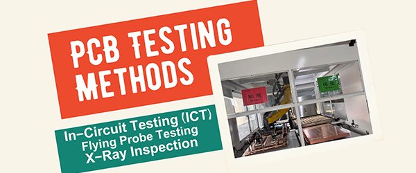
An Overview of PCB Testing Methods: ICT, Flying Probe, and X-Ray Inspection
Printed Circuit Boards (PCBs) are crucial to electronic devices, and their quality and reliability must be thoroughly tested before deployment. PCB testing methods such as In-Circuit Testing (ICT), Flying Probe Testing, and X-Ray Inspection help ensure that each board functions correctly, identifying potential defects and preventing failures. In this article, we’ll explore these three popular PCB testing methods, their unique benefits, limitations, and when each method is best suited for use.
Why PCB Testing Is Essential
PCB testing ensures the quality, performance, and longevity of electronic devices by identifying defects that could otherwise lead to functional failures. These defects may include short circuits, open circuits, component misalignment, and soldering issues. Effective testing reduces the risk of costly recalls, enhances reliability, and ensures customer satisfaction.
1. In-Circuit Testing (ICT)
What is ICT?
In-Circuit Testing (ICT) is a widely-used PCB testing method that employs a fixture with multiple probes (or “bed of nails”) to make electrical contact with specific points on the board. The ICT machine sends signals through the PCB and measures responses, verifying connections, component placement, and functionality.
Benefits of ICT:
High Accuracy and Coverage: ICT can detect a wide range of issues, including component values, open/short circuits, and soldering defects.
Quick Testing for High Volumes: ICT is highly efficient, making it ideal for large-scale production lines.
Limitations of ICT:
High Initial Cost: ICT requires a custom test fixture, which can be expensive to design and manufacture.
Less Flexible: Changes in PCB design require new fixtures, increasing time and cost.
Best for: High-volume production of simple to moderately complex PCBs with a stable design.
2. Flying Probe Testing
What is Flying Probe Testing?
Flying Probe Testing uses multiple probes that move across the PCB to make contact with test points, checking for correct connections, short circuits, and component placement. Unlike ICT, flying probe testing does not require a custom fixture, making it more adaptable to changes in PCB design.
Benefits of Flying Probe Testing:
Cost-Effective for Low Volumes: Flying probe testing is ideal for low-volume production or prototypes as it doesn’t require a fixture.
Flexibility: Design changes can be easily accommodated without the need for new hardware.
Limitations of Flying Probe Testing:
Longer Test Times: Flying probe testing is slower than ICT, which can limit its suitability for high-volume production.
Limited Coverage: Flying probes may not detect all possible defects, especially in complex PCBs.
Best for: Prototype testing, low- to medium-volume production, and complex PCBs with frequent design changes.
3. X-Ray Inspection
What is X-Ray Inspection?
X-Ray Inspection, also known as Automated X-Ray Inspection (AXI), is a non-invasive testing method that uses X-rays to inspect the internal structure of a PCB. This method allows testers to view hidden connections, such as those under BGAs (Ball Grid Arrays), and check for defects like voids, soldering issues, and component misalignment.
Benefits of X-Ray Inspection:
Non-Invasive and Thorough: X-Ray inspection reveals hidden defects that are undetectable by ICT and flying probe testing.
Ideal for Complex Assemblies: X-Ray inspection can effectively test multilayer boards and high-density layouts with complex connections.
Limitations of X-Ray Inspection:
High Cost: X-Ray inspection equipment is expensive, making it less feasible for low-budget projects.
Skill Requirement: Skilled operators are often needed to interpret the results accurately.
Best for: Complex PCBs with hidden solder joints, BGAs, and high-density assemblies.
Comparison of ICT, Flying Probe, and X-Ray Testing
Below is a table that compares In-Circuit Testing (ICT), Flying Probe Testing, and X-Ray Inspection based on key factors such as cost, testing speed, and best use cases.
Feature | In-Circuit Testing (ICT) | Flying Probe Testing | X-Ray Inspection |
Setup Cost | High (due to custom fixture) | Low to Moderate | High |
Testing Speed | Fast, ideal for high volumes | Slower, best for low volumes | Moderate |
Flexibility | Low, requires new fixture for design changes | High, adaptable to design changes | Moderate, but requires operator skill |
Defect Detection | High coverage, ideal for connectivity | Good for general defects | Excellent for hidden defects (e.g., BGAs) |
Best for | High-volume production | Low- to medium-volume, prototypes | High-density, complex boards |
Applications | Consumer electronics, automotive | Prototyping, low-volume manufacturing | Medical devices, aerospace, and high-density PCBs |
Choosing the Right PCB Testing Method
Selecting the appropriate PCB testing method depends on various factors, including production volume, design complexity, and budget. Here’s a summary to help guide the decision:
In-Circuit Testing (ICT): Best for high-volume production and stable designs. Its accuracy and speed make it ideal for simpler PCBs where custom fixtures are feasible.
Flying Probe Testing: Most suitable for prototyping and low-to-medium volume production, especially when designs may change frequently. This method is cost-effective without the need for custom fixtures.
X-Ray Inspection: Best for complex, high-density PCBs with hidden connections. X-Ray is also ideal for critical applications like medical devices and aerospace where hidden defects can be catastrophic.
Combining these methods can be beneficial for large-scale production where both flexibility and thorough defect detection are necessary.
Choosing the right PCB testing method—whether ICT, flying probe, or X-ray inspection—depends on the unique needs of your project. Each method has distinct advantages and limitations, and understanding these differences can optimize production quality, cost, and reliability. For low-volume or prototype testing, flying probe testing offers flexibility without high costs, while ICT provides rapid testing for high-volume production. For complex, multilayered boards with hidden connections, X-ray inspection offers the thoroughness needed to ensure reliability and functionality.
Choosing the right PCB testing method—whether ICT, flying probe, or X-ray inspection—depends on the unique needs of your project. Each method has distinct advantages and limitations, and understanding these differences can optimize production quality, cost, and reliability. For low-volume or prototype testing, flying probe testing offers flexibility without high costs, while ICT provides rapid testing for high-volume production. For complex, multilayered boards with hidden connections, X-ray inspection offers the thoroughness needed to ensure reliability and functionality.