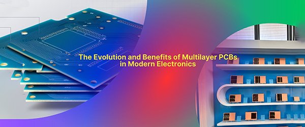
The Evolution and Benefits of Multilayer PCBs in Modern Electronics
As technology advances, electronic devices are becoming increasingly compact, versatile, and powerful. The demand for sophisticated devices has led to the development of complex circuit boards that can meet the high standards of today’s tech applications. One of the pivotal components in this evolution is the Multilayer Printed Circuit Board (PCB).
Multilayer PCBs have become the standard for high-performance electronic devices, offering increased functionality within a reduced space. In this article, we will explore the structure, benefits, applications, and future prospects of multilayer PCBs in modern electronics.
What is a Multilayer PCB?
A Multilayer PCB is a circuit board with three or more layers of conductive material stacked together, separated by insulating layers, or prepreg. This stacked configuration enables the creation of complex circuits within a smaller footprint. While single-layer and double-layer PCBs consist of only one or two conductive layers, multilayer PCBs typically contain at least three, with many advanced designs having up to 50 layers or more. Each layer is connected via vias—small holes filled with conductive material that facilitate signal flow between layers.
The layers are pressed together with heat and adhesive, creating a robust, compact structure that houses more components and pathways in a smaller area compared to single- or double-layer boards.
Key Benefits of Multilayer PCBs
--- Higher Density and Reduced Size Multilayer PCBs enable high-density circuit designs by utilizing vertical space rather than just surface area. This capability allows designers to incorporate more complex circuits into smaller spaces, making these boards ideal for compact and portable devices such as smartphones, laptops, and wearables.
--- Enhanced Performance Because multilayer PCBs have multiple layers of conductive traces, they provide lower resistance and inductance than single-layer PCBs. This results in faster signal transmission and enhanced electrical performance, especially beneficial for high-frequency circuits and high-speed data transfer applications.
--- Greater Durability The structure of multilayer PCBs offers inherent durability due to the added layers, which reinforce each other, creating a more robust and resilient circuit board. This increased durability is especially important in industrial and military applications, where devices are exposed to harsh conditions.
--- Improved Signal Integrity The closely packed layers reduce the length of interconnections, which minimizes noise and interference. Multilayer boards also enable the inclusion of dedicated ground and power planes, providing better shielding and power distribution across the board. These features are crucial for high-speed, high-frequency applications, where signal integrity is paramount.
--- Design Flexibility Multilayer PCBs offer more design flexibility than single- or double-sided boards. Engineers can use the extra layers to route complex circuits while keeping the board size compact. This flexibility is essential for creating innovative and multifunctional electronic products.
Common Applications of Multilayer PCBs
Multilayer PCBs are widely used across various industries due to their compact size, high performance, and reliability. Some common applications include:
--- Consumer Electronics: Smartphones, laptops, and tablets rely on multilayer PCBs to integrate multiple functions and provide high-speed performance in a small package.
--- Automotive Electronics: Advanced driver-assistance systems (ADAS), in-car infotainment, and engine control systems often use multilayer PCBs for their processing power and reliability.
--- Telecommunications: Network infrastructure and communication devices benefit from multilayer PCBs' ability to handle high-frequency signals and complex routing.
--- Medical Devices: Equipment such as imaging systems, monitors, and portable medical devices use multilayer PCBs for their precision and reliability.
--- Aerospace and Defense: Multilayer PCBs meet the stringent requirements for performance and durability in aerospace and defense applications, including radar, navigation, and control systems.
Manufacturing Process for Multilayer PCBs
The manufacturing of multilayer PCBs is a complex process that requires precise control at each step:
--- Layer Preparation – Individual layers are created with conductive material and undergo etching to form the circuit patterns.
--- Layer Stacking – These layers are stacked with insulating layers (prepreg) in between and are aligned carefully to ensure accurate connections.
--- Lamination – The stacked layers are laminated together under heat and pressure, forming a single, unified structure.
--- Drilling and Plating – Holes are drilled through the board to create vias, which are then plated with a conductive material to establish electrical connections between layers.
--- Testing – Final testing checks for electrical continuity, insulation resistance, and overall functionality to ensure the board meets design specifications.
Future Prospects and Trends in Multilayer PCBs
As technology continues to evolve, the role of multilayer PCBs is expected to expand, especially with the growth of 5G, Internet of Things (IoT), and Artificial Intelligence (AI) applications. Future trends for multilayer PCBs include:
--- Higher Layer Counts: With advancements in fabrication techniques, PCBs with more than 50 layers are becoming viable for ultra-complex applications.
--- Flexible Multilayer PCBs: Flex and rigid-flex multilayer boards are increasingly used in applications where traditional rigid PCBs cannot fit, such as in wearable devices and foldable smartphones.
--- Advanced Materials: The use of advanced substrates like polyimide and Teflon is increasing, especially for high-speed and high-frequency applications where standard FR4 materials may not be sufficient.
Multilayer PCBs represent a significant advancement in circuit board technology, enabling the development of compact, high-performance electronic devices. Their ability to support complex, high-density circuits in small spaces makes them indispensable in industries ranging from consumer electronics to aerospace. As we look to the future, multilayer PCBs will continue to be a cornerstone of innovation, supporting the next generation of smart, connected, and powerful devices.